
Insider Brief
- MIT researchers have developed a fully autonomous robotic system that can perform over 3,000 precise photoconductance measurements in 24 hours, a key for accelerating semiconductor material discovery.
- Backed by funding from the U.S. Department of Energy, National Science Foundation, First Solar, and others, the robot combines a self-supervised neural network and domain-informed path planning to optimize speed and accuracy.
- The system automates a traditionally slow and manual process, enabling faster identification of promising solar cell materials and laying groundwork for future fully autonomous materials labs.
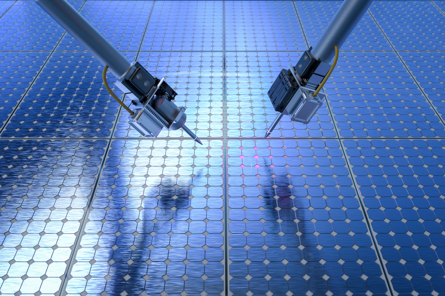
A research team at MIT has built a fully autonomous robotic system that can rapidly and precisely measure photoconductance, an essential electrical property in new semiconductor materials.
With funding from the U.S. Department of Energy, the National Science Foundation, First Solar, and other industry partners, the robotic probe, guided by a self-supervised neural network and domain-informed planning software, performed more than 3,000 unique measurements in a 24-hour test, significantly outpacing existing AI-based tools.
“Not every important property of a material can be measured in a contactless way. If you need to make contact with your sample, you want it to be fast and you want to maximize the amount of information that you gain,” noted Tonio Buonassisi, professor of mechanical engineering and senior author of the study.
According to MIT, the system was developed to address the slow pace of materials discovery in applications like solar panels, where finding more efficient semiconductors is critical. Photoconductance, which measures how well a material conducts electricity when exposed to light, is a key benchmark for photovoltaic performance. Measuring it typically requires human-operated probes and is time-consuming, especially across irregularly shaped samples like perovskites. MIT’s new robot automates that process and makes it faster, more reliable, and more detailed.
The platform uses an onboard camera to scan the sample and then employs computer vision to divide the image into segments. These are analyzed by a neural network that integrates materials science knowledge to determine where the probe should make contact to collect the most informative data. A path-planning algorithm then calculates the most efficient route for the robot to travel between measurement points.
Researchers indicated this approach not only reduced computation time compared to seven other AI models but also produced shorter measurement paths. By introducing minor randomness into the route-planning algorithm, they improved path efficiency. The robot’s flexible, self-supervised system requires no labeled training data, allowing it to adapt to novel material shapes without human intervention.
Results showed more than 125 photoconductance readings per hour, with improved detection of subtle material features, including performance hotspots and early signs of degradation. The technology could streamline semiconductor screening and accelerate the development of next-generation solar materials.
Co-authors of the study include lead author Alexander (Aleks) Siemenn, a graduate student; postdocs Basita Das and Kangyu Ji; and graduate student Fang Sheng. The work appears in Science Advances.
“These robots can improve the repeatability and precision of our operations, but it is important to still have a human in the loop. If we don’t have a good way to implement the rich knowledge from these chemical experts into our robots, we are not going to be able to discover new materials,” Siemenn adds.
The team aims to extend the system’s capabilities and develop a complete automated lab that combines synthesis, imaging, and measurement.
The project also received funding from Eni (through the MIT Energy Initiative), MathWorks, and the University of Toronto’s Acceleration Consortium.