
Insider Brief
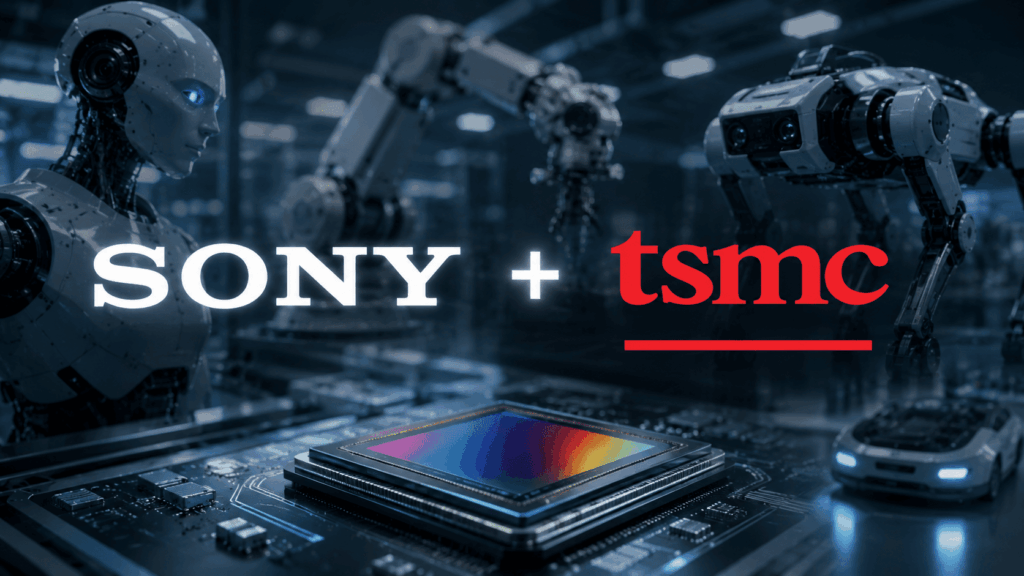
- Sony Semiconductor Solutions and TSMC announced plans to form a strategic partnership focused on developing next-generation image sensors for robotics, automotive systems and physical AI applications.
- The companies signed a non-binding memorandum of understanding to establish a joint venture that would create new development and production lines at Sony’s semiconductor facility in Kumamoto Prefecture, Japan, with Sony holding a controlling stake.
- The partnership combines Sony’s image sensor expertise with TSMC’s semiconductor manufacturing capabilities as demand grows for advanced sensing systems designed to support increasingly autonomous machines and AI-driven perception systems.
Sony Semiconductor Solutions and Taiwan Semiconductor Manufaccturing Company announced a plan to form a strategic partnership focused on developing and manufacturing next-generation image sensors, with the companies highlighting future applications in robotics, automotive systems and physical AI.
According to a joint press release, the companies signed a non-binding memorandum of understanding to create a joint venture that would establish new development and production lines at Sony’s semiconductor facility in Kumamoto Prefecture, Japan. Sony would hold a controlling stake in the venture.
The partnership combines Sony’s image sensor design capabilities with TSMC’s semiconductor manufacturing and process technologies as demand grows for advanced sensing systems capable of supporting increasingly autonomous machines.
“This JV is a significant initiative that brings together the strengths of both companies and aims to drive further advancement in technology and business within the next-generation image sensor field,” Shinji Sashida, CEO and president of Sony Semiconductor Solutions, said in the announcement. “Building on this JV, Sony intends to further strengthen its business operations with a focus on creating high added value.”
Sony Semiconductor Solutions, a wholly-owned subsidiary of Sony, and TSMC are also evaluating additional investments tied to the venture and Sony’s existing facilities in Nagasaki, with implementation expected to occur in phases based on market demand and potential support from the Japanese government.
“Sony has been our long-time partner in the CMOS image sensor business,” noted TSMC Senior Vice President and Deputy Co-COO, Dr. Kevin Zhang. “We are excited to elevate our collaboration to the next level, which represents a key step forward in driving future sensing technology in the AI era. This partnership underscores our shared commitment and mutual vision of leveraging cutting-edge technologies and innovative solutions to deliver leading sensing technology and products.”